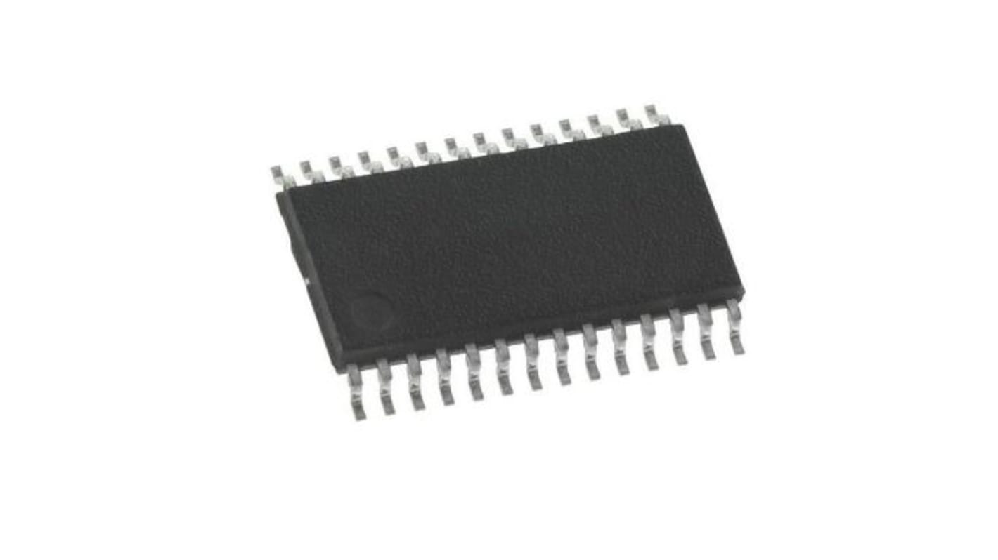
Renesas Electronics 9DB433AGLF Clock Buffer 28-Pin TSSOP
- RS Stock No.:
- 216-6246
- Mfr. Part No.:
- 9DB433AGLF
- Manufacturer:
- Renesas Electronics

This image is representative of the product range
Subtotal (1 tube of 50 units)*
PHP14,259.70
(exc. VAT)
PHP15,970.85
(inc. VAT)
FREE delivery for orders over ₱3,000.00
Temporarily out of stock
- Shipping from June 03, 2026
Need more? Click ‘Check delivery dates’ to find extra stock and lead times.
Units | Per Unit | Per Tube* |
|---|---|---|
| 50 + | PHP285.194 | PHP14,259.70 |
*price indicative
- RS Stock No.:
- 216-6246
- Mfr. Part No.:
- 9DB433AGLF
- Manufacturer:
- Renesas Electronics
Specifications
Technical data sheets
Legislation and Compliance
Product Details
Find similar products by selecting one or more attributes.
Select all | Attribute | Value |
|---|---|---|
| Brand | Renesas Electronics | |
| Product Type | Clock Buffer | |
| Maximum Input Frequency | 166MHz | |
| Mount Type | Surface | |
| Maximum Propagation Delay Time | 150ps | |
| Package Type | TSSOP | |
| Pin Count | 28 | |
| Number of Outputs | 12 | |
| Minimum Supply Voltage | 3.3V | |
| Maximum Supply Voltage | 4.6V | |
| Minimum Operating Temperature | 0°C | |
| Maximum Operating Temperature | 70°C | |
| Width | 6.2 mm | |
| Series | 9DB | |
| Standards/Approvals | No | |
| Height | 1.2mm | |
| Length | 17.1mm | |
| Automotive Standard | No | |
| Select all | ||
|---|---|---|
Brand Renesas Electronics | ||
Product Type Clock Buffer | ||
Maximum Input Frequency 166MHz | ||
Mount Type Surface | ||
Maximum Propagation Delay Time 150ps | ||
Package Type TSSOP | ||
Pin Count 28 | ||
Number of Outputs 12 | ||
Minimum Supply Voltage 3.3V | ||
Maximum Supply Voltage 4.6V | ||
Minimum Operating Temperature 0°C | ||
Maximum Operating Temperature 70°C | ||
Width 6.2 mm | ||
Series 9DB | ||
Standards/Approvals No | ||
Height 1.2mm | ||
Length 17.1mm | ||
Automotive Standard No | ||
The Renesas Electronics 9DB433 zero-delay buffer supports PCIe Gen3 requirements, while being backwards compatible to PCIe Gen2 and Gen1. The 9DB433 is driven by a differential SRC output pair from an IDT 932S421 or 932SQ420 or equivalent main clock generator.
Output cycle-cycle jitter <50ps
Output to Output skew <50ps
Phase jitter: PCIe Gen3 <1.0ps rms
Related links
- Renesas Electronics 9DB433AGLF Clock Buffer 28-Pin TSSOP-28
- Renesas Electronics 9DB433AGILF Clock Buffer 28-Pin TSSOP-28
- Renesas Electronics 9DB403DGLFT Clock Buffer 28-Pin TSSOP-28
- Renesas Electronics 9DB633AGILF Clock Buffer 28-Pin TSSOP
- Renesas Electronics 9DB106BGILFT PLL Clock Buffer 28-Pin 28-pin TSSOP
- Renesas Electronics 9DB106BGLF Clock Buffer 28-Pin TSSOP
- Renesas Electronics 9DB106BGLFT Buffer 28-Pin TSSOP
- Renesas Electronics 9DB403DFLFT PLL Clock Buffer 28-Pin 28-pin SSOP
