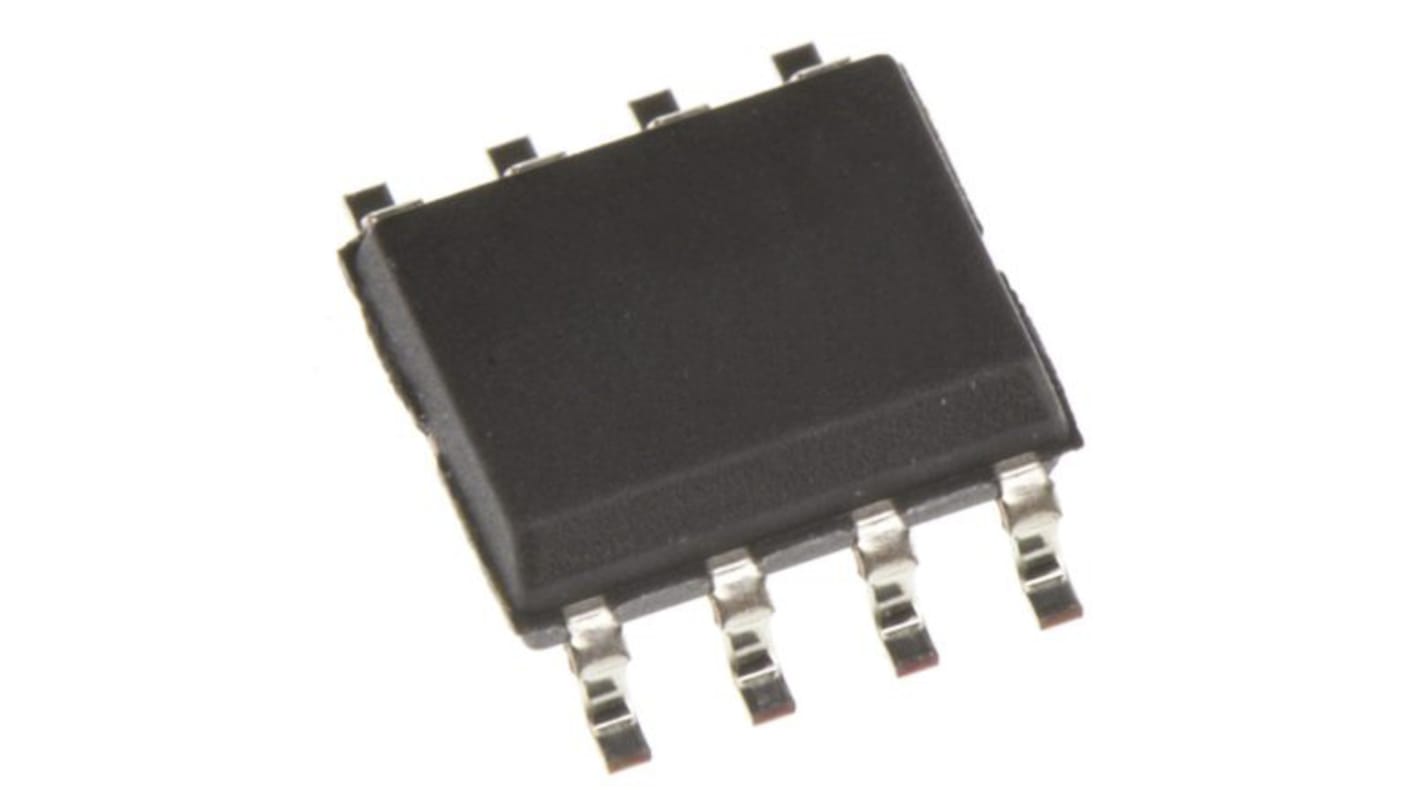
onsemi, Logic Level Translator Translator 2 ECL to LVTTL, 8-Pin SOIC
- RS Stock No.:
- 186-8831
- Mfr. Part No.:
- MC100EPT25DG
- Manufacturer:
- onsemi

Bulk discount available
Subtotal (1 tube of 98 units)*
PHP76,985.664
(exc. VAT)
PHP86,223.928
(inc. VAT)
FREE delivery for orders over ₱3,000.00
In Stock
- 1,666 unit(s) ready to ship from another location
Need more? Click ‘Check delivery dates’ to find extra stock and lead times.
Units | Per Unit | Per Tube* |
|---|---|---|
| 98 - 98 | PHP785.568 | PHP76,985.66 |
| 196 - 392 | PHP731.938 | PHP71,729.92 |
| 490 - 686 | PHP709.788 | PHP69,559.22 |
| 784 - 882 | PHP665.928 | PHP65,260.94 |
| 980 + | PHP664.375 | PHP65,108.75 |
*price indicative
- RS Stock No.:
- 186-8831
- Mfr. Part No.:
- MC100EPT25DG
- Manufacturer:
- onsemi
Specifications
Technical data sheets
Legislation and Compliance
Product Details
Find similar products by selecting one or more attributes.
Select all | Attribute | Value |
|---|---|---|
| Brand | onsemi | |
| Logic Family | ECL | |
| Product Type | Logic Level Translator | |
| Direction Type | Uni-Directional | |
| Maximum Propagation Delay Time @ CL | 2ns | |
| Mount Type | Surface | |
| Package Type | SOIC | |
| Number of Elements per Chip | 2 | |
| Pin Count | 8 | |
| Output Type | LVTTL | |
| Logic Function | Translator | |
| Maximum Low Level Output Current | 24mA | |
| Maximum High Level Output Current | -3mA | |
| Minimum Supply Voltage | 3V | |
| Maximum Supply Voltage | 3.6V | |
| Translation | ECL to LVTTL | |
| Minimum Operating Temperature | -40°C | |
| Maximum Operating Temperature | 85°C | |
| Length | 5mm | |
| Standards/Approvals | No | |
| Series | MC100EPT2 | |
| Height | 1.5mm | |
| Automotive Standard | No | |
| Select all | ||
|---|---|---|
Brand onsemi | ||
Logic Family ECL | ||
Product Type Logic Level Translator | ||
Direction Type Uni-Directional | ||
Maximum Propagation Delay Time @ CL 2ns | ||
Mount Type Surface | ||
Package Type SOIC | ||
Number of Elements per Chip 2 | ||
Pin Count 8 | ||
Output Type LVTTL | ||
Logic Function Translator | ||
Maximum Low Level Output Current 24mA | ||
Maximum High Level Output Current -3mA | ||
Minimum Supply Voltage 3V | ||
Maximum Supply Voltage 3.6V | ||
Translation ECL to LVTTL | ||
Minimum Operating Temperature -40°C | ||
Maximum Operating Temperature 85°C | ||
Length 5mm | ||
Standards/Approvals No | ||
Series MC100EPT2 | ||
Height 1.5mm | ||
Automotive Standard No | ||
The MC100EPT25 is a Differential LVECL/ECL to LVTTL translator. This device requires +3.3V, -3.3V to -5.2V, and ground. The small outline 8-lead SOIC package and the single gate of the EPT25 make it ideal for applications which require the translation of a clock or data signal.
The VBB output allows the EPT25 to also be used in a single-ended input mode. In this mode the VBB output is tied to the D input for a inverting buffer or the D input for a non-inverting buffer. If used, the VBB pin should be bypassed to ground with at least a 0.01 μF capacitor.
1.1ns Typical Propagation Delay
Maximum Frequency > 275 MHz Typical
Operating Range: VCC = 3.0 V to 3.6 V, VEE = -5.5 V to -3.0 V, GND = 0 V
24mA TTL outputs
Q Output will default LOW with inputs open or at GND
VBB Output
Open Input Default State
Safety Clamp on Inputs
Pb-Free Packages are Available
