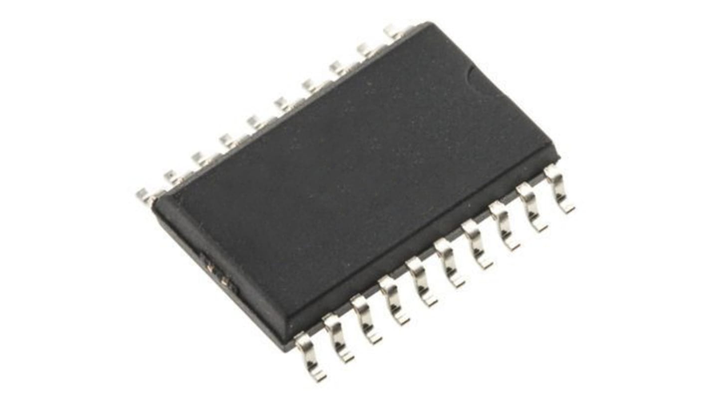
onsemi MC74HCT573ADWG, Voltage Level Translator Latch 1 TTL/NMOS, 20-Pin SOIC
- RS Stock No.:
- 186-8300
- Mfr. Part No.:
- MC74HCT573ADWG
- Manufacturer:
- onsemi

This image is representative of the product range
Subtotal (1 pack of 25 units)*
PHP1,020.175
(exc. VAT)
PHP1,142.60
(inc. VAT)
Stock information currently inaccessible - Please check back later
Units | Per Unit | Per Pack* |
|---|---|---|
| 25 + | PHP40.807 | PHP1,020.18 |
*price indicative
- RS Stock No.:
- 186-8300
- Mfr. Part No.:
- MC74HCT573ADWG
- Manufacturer:
- onsemi
Specifications
Technical data sheets
Legislation and Compliance
Product Details
Find similar products by selecting one or more attributes.
Select all | Attribute | Value |
|---|---|---|
| Brand | onsemi | |
| Product Type | Voltage Level Translator | |
| Direction Type | Bi-Directional | |
| Logic Family | HCT | |
| Maximum Propagation Delay Time @ CL | 45ns | |
| Mount Type | Surface | |
| Package Type | SOIC | |
| Number of Elements per Chip | 1 | |
| Pin Count | 20 | |
| Output Type | 3 State | |
| Logic Function | Latch | |
| Maximum Low Level Output Current | 6mA | |
| Minimum Supply Voltage | 4.5V | |
| Maximum High Level Output Current | 6mA | |
| Translation | TTL/NMOS | |
| Maximum Supply Voltage | 5.5V | |
| Minimum Operating Temperature | -55°C | |
| Maximum Operating Temperature | 125°C | |
| Standards/Approvals | No | |
| Series | MC74HCT573 | |
| Height | 2.4mm | |
| Length | 12.95mm | |
| Automotive Standard | No | |
| Select all | ||
|---|---|---|
Brand onsemi | ||
Product Type Voltage Level Translator | ||
Direction Type Bi-Directional | ||
Logic Family HCT | ||
Maximum Propagation Delay Time @ CL 45ns | ||
Mount Type Surface | ||
Package Type SOIC | ||
Number of Elements per Chip 1 | ||
Pin Count 20 | ||
Output Type 3 State | ||
Logic Function Latch | ||
Maximum Low Level Output Current 6mA | ||
Minimum Supply Voltage 4.5V | ||
Maximum High Level Output Current 6mA | ||
Translation TTL/NMOS | ||
Maximum Supply Voltage 5.5V | ||
Minimum Operating Temperature -55°C | ||
Maximum Operating Temperature 125°C | ||
Standards/Approvals No | ||
Series MC74HCT573 | ||
Height 2.4mm | ||
Length 12.95mm | ||
Automotive Standard No | ||
High-Performance Silicon-Gate CMOS
The MC74HCT573A is identical in pinout to the LS573. This device may be used as a level converter for interfacing TTL or NMOS outputs to High-Speed CMOS inputs.
These latches appear transparent to data (i.e., the outputs change asynchronously) when Latch Enable is high. When Latch Enable goes low, data meeting the setup and hold times becomes latched.
The Output Enable input does not affect the state of the latches, but when Output Enable is high, all device outputs are forced to the high-impedance state. Thus, data may be latched even when the outputs are not enabled.
The HCT573A is identical in function to the HCT373A but has the Data Inputs on the opposite side of the package from the outputs to facilitate PC board layout.
Output Drive Capability: 15 LSTTL Loads
TTL/CMOS-Compatible Input Levels
Outputs Directly Interface to CMOS, NMOS and TTL
Operating Voltage Range: 4.5 to 5.5 V
Low Input Current: 10 mA
Chip Complexity: 234 FETs or 58.5 Equivalent Gates
Improved Propagation Delays
50% Lower Quiescent Power
These devices are available in Pb-free package(s). Specifications herein apply to both standard and Pb-free devices
