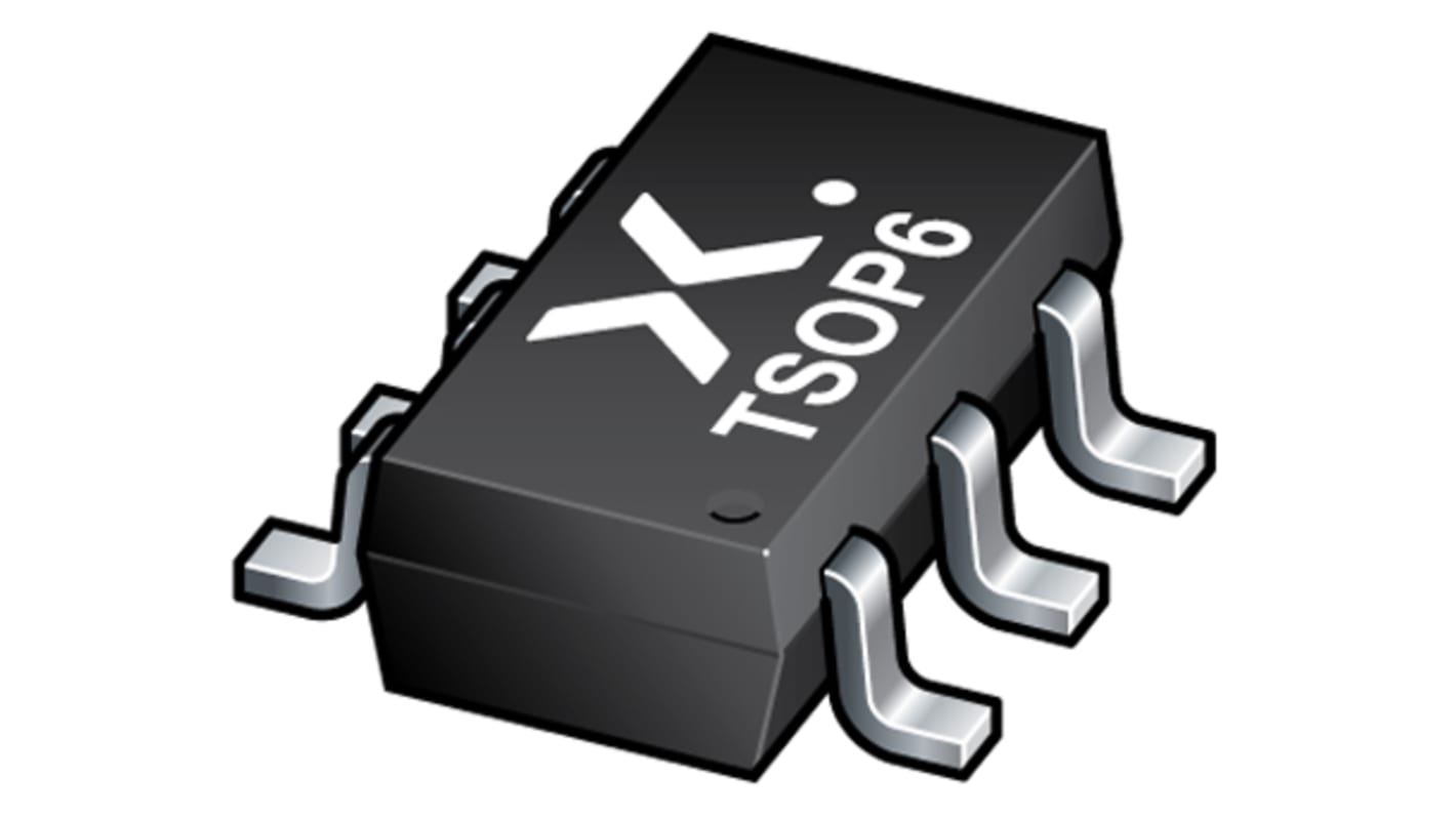
Nexperia 74LVC2G17GV,125 Dual Schmitt Trigger Inverter, 6-Pin TSOP

- RS Stock No.:
- 136-2153
- Mfr. Part No.:
- 74LVC2G17GV,125
- Manufacturer:
- Nexperia
Available for back order.
Added
Price Each (On a Reel of 3000)
PHP5.415
(exc. VAT)
PHP6.065
(inc. VAT)
| Units | Per Unit | Per Reel* |
| 3000 - 3000 | PHP5.415 | PHP16,245.00 |
| 6000 - 6000 | PHP4.914 | PHP14,742.00 |
| 9000 + | PHP4.497 | PHP13,491.00 |
| *price indicative | ||
- RS Stock No.:
- 136-2153
- Mfr. Part No.:
- 74LVC2G17GV,125
- Manufacturer:
- Nexperia
Technical data sheets
Legislation and Compliance
- COO (Country of Origin):
- MY
Product Details
Noisy signals? Get them clean with our Schmitt triggers. These devices are also useful for reshaping signals in complex layouts, and can prevent multiple switching when driven by slow edges. They feature a wide voltage supply range, input hysteresis, and CMOS and TTL variants
Prevents multiple switching when driven by slow edges
Cleans up the noisy signals
Reshapes the signals in complex layouts
Suitable for mixed 3.3 V and 5.0 V applications
Wide voltage supply range
Input hysteresis
Open drain output options
CMOS and TTL variants
Overvoltage tolerant input options
Cleans up the noisy signals
Reshapes the signals in complex layouts
Suitable for mixed 3.3 V and 5.0 V applications
Wide voltage supply range
Input hysteresis
Open drain output options
CMOS and TTL variants
Overvoltage tolerant input options
The 74LVC2G17 provides two non-inverting buffers with Schmitt trigger input. It is capable of transforming slowly changing input signals into sharply defined, jitter-free output signals.Inputs can be driven from either 3.3 V or 5 V devices. This feature allows the use of these devices as translators in a mixed 3.3 V and 5 V environment.This device is fully specified for partial power-down applications using IOFF. The IOFF circuitry disables the output, preventing the damaging backflow current through the device when it is powered down
Wide supply voltage range from 1.65 V to 5.5 V
5 V tolerant input/output for interfacing with 5 V logic
High noise immunity
Complies with JEDEC standard:
JESD8-7 (1.65 V to 1.95 V)
JESD8-5 (2.3 V to 2.7 V)
JESD-8B/JESD36 (2.7 V to 3.6 V)
ESD protection:
HBM JESD22-A114F exceeds 2000 V
MM JESD22-A115-A exceeds 200 V
24 mA output drive (VCC =3.0V)
CMOS low-power consumption
Latch-up performance exceeds 250 mA
Direct interface with TTL levels
Multiple package options
Specified from 40 Cto+85 C and 40 Cto+125 C
Specifications
Attribute | Value |
|---|---|
| Logic Function | Non-Inverting |
| Input Type | Schmitt Trigger |
| Output Type | TTL |
| Number of Elements per Chip | 2 |
| Schmitt Trigger Input | Yes |
| Maximum Propagation Delay Time @ Maximum CL | 13.1 ns @ 1.95 V |
| Mounting Type | Surface Mount |
| Package Type | TSOP |
| Pin Count | 6 |
| Logic Family | 74LVC |
| Dimensions | 3.1 x 1.7 x 1mm |
| Maximum Operating Supply Voltage | 5.5 V |
| Height | 1mm |
| Length | 3.1mm |
| Minimum Operating Temperature | -40 °C |
| Minimum Operating Supply Voltage | 1.65 V |
| Maximum Operating Temperature | +125 °C |
| Width | 1.7mm |