Infineon Isolated HEXFET 2 Type N-Channel MOSFET, 3 A, 50 V Enhancement, 8-Pin SOIC IRF7103TRPBF
- RS Stock No.:
- 831-2865
- Distrelec Article No.:
- 304-44-449
- Mfr. Part No.:
- IRF7103TRPBF
- Manufacturer:
- Infineon

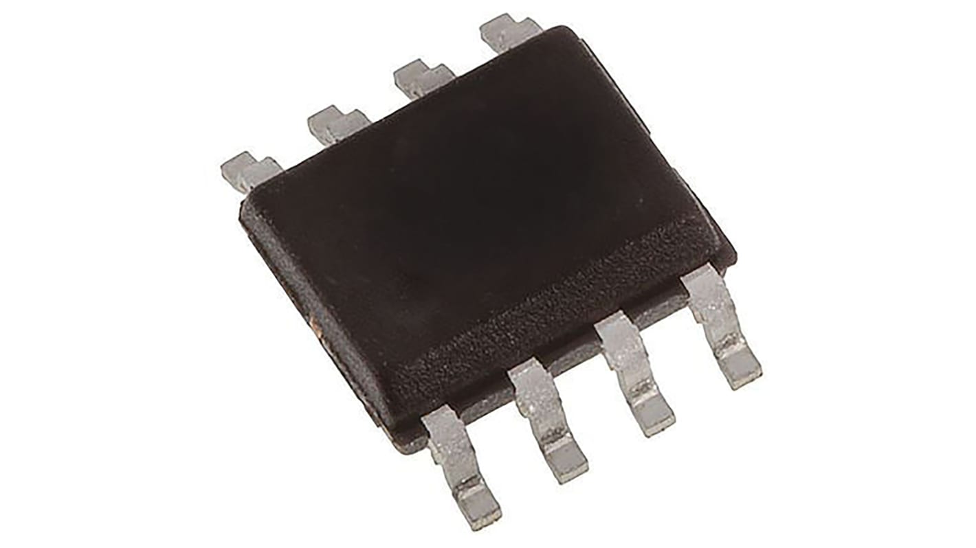
This image is representative of the product range
Bulk discount available
View bulk pricing optionsSubtotal (1 pack of 20 units)*
PHP780.28
(exc. VAT)
PHP873.92
(inc. VAT)
FREE delivery for orders over ₱3,000.00
In Stock
- Plus 2,380 unit(s) shipping from July 20, 2026
- Plus 4,560 unit(s) shipping from July 27, 2026
Need more? Click ‘Check delivery dates’ to find extra stock and lead times.
Units | Per Unit | Per Pack* |
|---|---|---|
| 20 - 20 | PHP39.014 | PHP780.28 |
| 40 - 80 | PHP37.843 | PHP756.86 |
| 100 - 180 | PHP36.708 | PHP734.16 |
| 200 - 380 | PHP35.607 | PHP712.14 |
| 400 + | PHP34.538 | PHP690.76 |
*price indicative
- RS Stock No.:
- 831-2865
- Distrelec Article No.:
- 304-44-449
- Mfr. Part No.:
- IRF7103TRPBF
- Manufacturer:
- Infineon
Specifications
Technical data sheets
Legislation and Compliance
Product Details
Find similar products by selecting one or more attributes.
Select all | Attribute | Value |
|---|---|---|
| Brand | Infineon | |
| Channel Type | Type N | |
| Product Type | MOSFET | |
| Maximum Continuous Drain Current Id | 3A | |
| Maximum Drain Source Voltage Vds | 50V | |
| Package Type | SOIC | |
| Series | HEXFET | |
| Mount Type | Surface | |
| Pin Count | 8 | |
| Maximum Drain Source Resistance Rds | 200mΩ | |
| Channel Mode | Enhancement | |
| Forward Voltage Vf | 1.2V | |
| Maximum Power Dissipation Pd | 2W | |
| Minimum Operating Temperature | -55°C | |
| Typical Gate Charge Qg @ Vgs | 12nC | |
| Transistor Configuration | Isolated | |
| Maximum Operating Temperature | 150°C | |
| Standards/Approvals | No | |
| Length | 5mm | |
| Height | 1.5mm | |
| Number of Elements per Chip | 2 | |
| Automotive Standard | No | |
| Select all | ||
|---|---|---|
Brand Infineon | ||
Channel Type Type N | ||
Product Type MOSFET | ||
Maximum Continuous Drain Current Id 3A | ||
Maximum Drain Source Voltage Vds 50V | ||
Package Type SOIC | ||
Series HEXFET | ||
Mount Type Surface | ||
Pin Count 8 | ||
Maximum Drain Source Resistance Rds 200mΩ | ||
Channel Mode Enhancement | ||
Forward Voltage Vf 1.2V | ||
Maximum Power Dissipation Pd 2W | ||
Minimum Operating Temperature -55°C | ||
Typical Gate Charge Qg @ Vgs 12nC | ||
Transistor Configuration Isolated | ||
Maximum Operating Temperature 150°C | ||
Standards/Approvals No | ||
Length 5mm | ||
Height 1.5mm | ||
Number of Elements per Chip 2 | ||
Automotive Standard No | ||
- COO (Country of Origin):
- PH
Infineon HEXFET Series MOSFET, 3A Maximum Continuous Drain Current, 2W Maximum Power Dissipation - IRF7103TRPBF
This MOSFET is designed for efficient performance across various applications. Its Durable construction is particularly beneficial in circuits requiring effective power management, making it suitable for electrical and automation sectors. With a maximum drain-source voltage of 50V, it ensures reliable switching capabilities to meet application demands.
Features & Benefits
• Low Rds(on) of 200mΩ for improved efficiency
• Maximum continuous drain current of 3A enhances power handling
• Operational temperatures up to +150°C for increased reliability
• Wide gate threshold range of 1V to 3V for flexible control
• Dual isolated transistor configuration aids circuit integration
• Surface mount design simplifies PCB assembly and optimises space
Applications
• Used in power supply designs for energy-efficient operation
• Integrated into motor drive for efficient motor control
• Employed in switching power supplies for improved performance
• Suitable for automation systems needing dependable switching components
What is the recommended operating temperature range for this component?
The component operates efficiently within a temperature range of -55°C to +150°C, ensuring reliability in various environments.
How does one determine the suitable gate voltage for optimal performance?
The acceptable gate-source voltage varies from -20V to +20V, providing flexibility in control circuit designs. For best results, operating near 10V is recommended, as indicated by typical gate charge specifications.
What safety precautions should be taken when using this device?
It is important to not exceed the voltage and current ratings during operation to avoid potential failure or damage. Moreover, appropriate heatsinking may be necessary to maintain optimal operating temperatures under heavy loads.
Can it be used in circuits requiring fast switching?
Yes, this MOSFET is designed for fast switching capabilities, making it well-suited for applications requiring high-speed performance, such as PWM control in motor drivers.
Is this MOSFET compatible with standard PCB layouts?
The surface mount design complies with standard PCB layouts, facilitating integration into existing circuits with minimal adjustments for placement.
Related links
- Infineon Isolated HEXFET 2 Type N-Channel MOSFET 50 V Enhancement, 8-Pin SOIC
- Infineon Isolated HEXFET 2 Type P 3.5 A 8-Pin SOIC
- Infineon Isolated HEXFET 2 Type P 3.5 A 8-Pin SOIC
- Infineon Isolated HEXFET 2 Type N 4 A 8-Pin SOIC
- Infineon Isolated HEXFET 2 Type N-Channel MOSFET 80 V Enhancement, 8-Pin SOIC
- Infineon Isolated HEXFET 2 Type N-Channel MOSFET 30 V Enhancement, 8-Pin SOIC
- Infineon Isolated HEXFET 2 Type P 3.5 A 8-Pin SOIC IRF7105TRPBF
- Infineon Isolated HEXFET 2 Type P 3.5 A 8-Pin SOIC IRF9952TRPBF