Infineon ISC Type N-Channel MOSFET, 230 A, 100 V, 8-Pin SuperSO8 5 x 6 ISC022N10NM6ATMA1
- RS Stock No.:
- 235-4862
- Mfr. Part No.:
- ISC022N10NM6ATMA1
- Manufacturer:
- Infineon

Bulk discount available
View bulk pricing optionsSubtotal (1 reel of 5000 units)*
PHP927,795.00
(exc. VAT)
PHP1,039,130.00
(inc. VAT)
FREE delivery for orders over ₱3,000.00
Temporarily out of stock
- 5,000 unit(s) shipping from August 20, 2026
Need more? Click ‘Check delivery dates’ to find extra stock and lead times.
Units | Per Unit | Per Reel* |
|---|---|---|
| 5000 - 5000 | PHP185.559 | PHP927,795.00 |
| 10000 - 10000 | PHP176.281 | PHP881,405.00 |
| 15000 + | PHP167.467 | PHP837,335.00 |
*price indicative
- RS Stock No.:
- 235-4862
- Mfr. Part No.:
- ISC022N10NM6ATMA1
- Manufacturer:
- Infineon
Specifications
Technical data sheets
Legislation and Compliance
Product Details
Find similar products by selecting one or more attributes.
Select all | Attribute | Value |
|---|---|---|
| Brand | Infineon | |
| Product Type | MOSFET | |
| Channel Type | Type N | |
| Maximum Continuous Drain Current Id | 230A | |
| Maximum Drain Source Voltage Vds | 100V | |
| Package Type | SuperSO8 5 x 6 | |
| Series | ISC | |
| Mount Type | Surface | |
| Pin Count | 8 | |
| Maximum Drain Source Resistance Rds | 2.24mΩ | |
| Typical Gate Charge Qg @ Vgs | 91nC | |
| Maximum Power Dissipation Pd | 245W | |
| Minimum Operating Temperature | -55°C | |
| Maximum Operating Temperature | 175°C | |
| Height | 5.1mm | |
| Standards/Approvals | No | |
| Length | 6.1mm | |
| Automotive Standard | No | |
| Select all | ||
|---|---|---|
Brand Infineon | ||
Product Type MOSFET | ||
Channel Type Type N | ||
Maximum Continuous Drain Current Id 230A | ||
Maximum Drain Source Voltage Vds 100V | ||
Package Type SuperSO8 5 x 6 | ||
Series ISC | ||
Mount Type Surface | ||
Pin Count 8 | ||
Maximum Drain Source Resistance Rds 2.24mΩ | ||
Typical Gate Charge Qg @ Vgs 91nC | ||
Maximum Power Dissipation Pd 245W | ||
Minimum Operating Temperature -55°C | ||
Maximum Operating Temperature 175°C | ||
Height 5.1mm | ||
Standards/Approvals No | ||
Length 6.1mm | ||
Automotive Standard No | ||
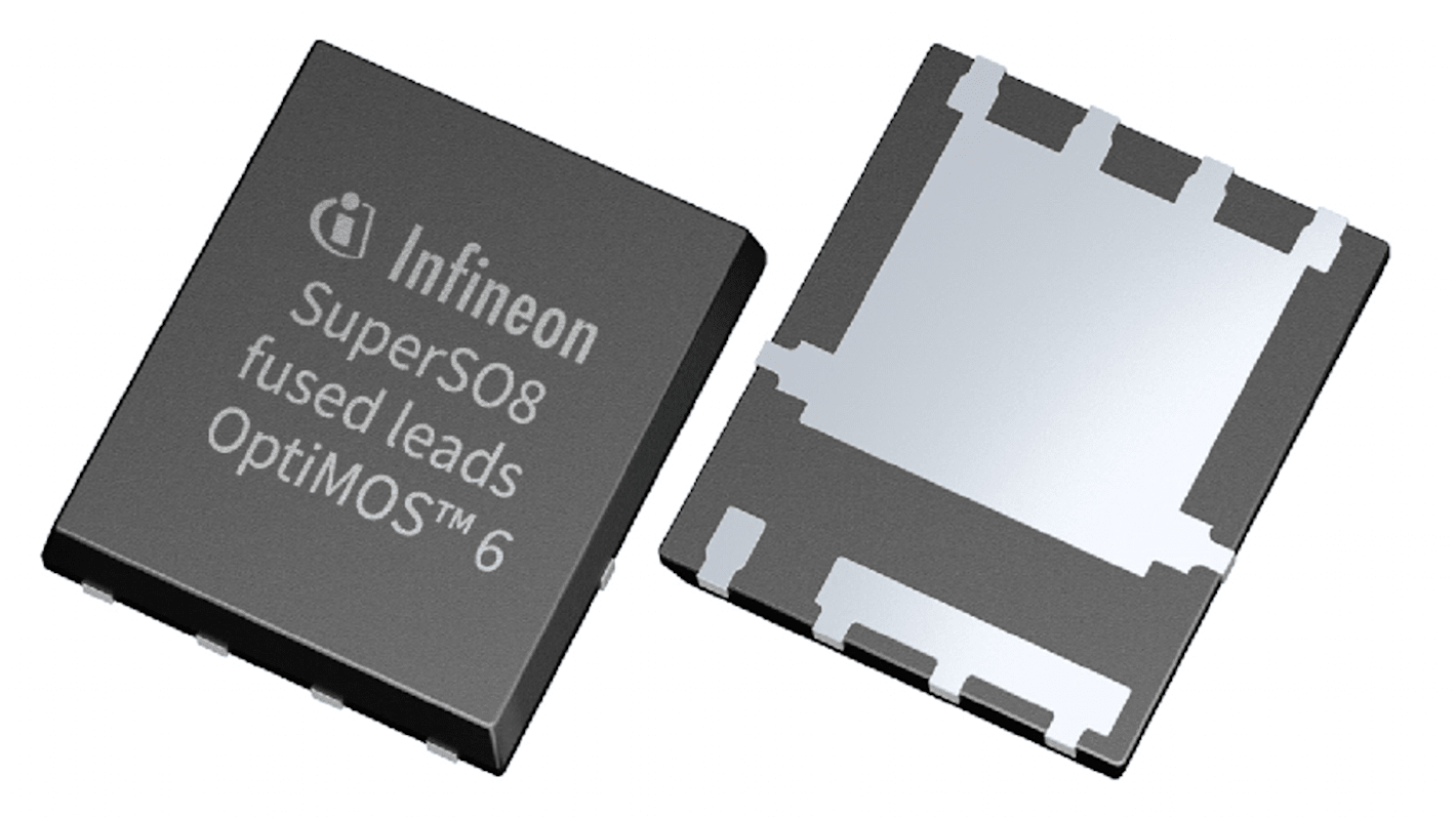
OptiMOS™ 6 power MOSFET 100 V Normal Level in SuperSO8 package
ISC022N10NM6 OptiMOS™ 6 100 V in normal level is setting the new technology standard in the field of discrete power MOSFETs. Compared to alternative products, Infineon’s leading thin wafer technology is enabling significant performance benefits.
Infineon’s OptiMOS™ 6 industrial power MOSFET 100 V is designed for high switching frequency application such as telecom and server power supply, but also the Ideal choice for other applications such as solar, power tools and drones.
In the SuperSO8 package it achieves ∼20% improvements in on-state resistance (RDS(on)) and 30% better figure of merits (FOM - RDS(on) x Qg and Qgd) compared to the previous technology OptiMOS™ 5. This enables designers to increase efficiency, allowing easier thermal design and less paralleling, leading to system cost reduction.
Summary of Features
Compared to OptiMOS™ 5, the new technology achieves:
•∼20% lower RDS(on)
•30% improved FOMg and 40% better FOMgd
•Lower and softer reverse recovery charge (Qrr)
•Ideal for high switching frequency
•MSL 1 classified according to J-STD-020
•175 °C junction temperature rating
•High avalanche energy rating
•Pb-free lead plating
•RoHS compliant
Benefits
•Low conduction losses
•Low switching losses
•Fast turn on and off
•Less paralleling required
•Robust reliable performance
•Environmentally friendly
•Less paralleling required
Related links
- Infineon ISC Type N-Channel MOSFET 100 V, 8-Pin SuperSO8 5 x 6 ISC022N10NM6ATMA1
- Infineon ISC Type N-Channel MOSFET 25 V, 8-Pin SuperSO8 5 x 6
- Infineon ISC Type N-Channel MOSFET 40 V, 8-Pin SuperSO8 5 x 6
- Infineon ISC Type N-Channel MOSFET 40 V, 8-Pin SuperSO8 5 x 6 ISC019N03L5SATMA1
- Infineon ISC Type N-Channel MOSFET 40 V, 8-Pin SuperSO8 5 x 6 ISC037N03L5ISATMA1
- Infineon ISC Type N-Channel MOSFET 25 V, 8-Pin SuperSO8 5 x 6 ISC010N06NM5
- Infineon BSC0 Type N-Channel MOSFET 40 V, 8-Pin SuperSO8 5 x 6
- Infineon IPZ Type N-Channel MOSFET 40 V, 8-Pin SuperSO8 5 x 6