Infineon C7 GOLD Type N-Channel MOSFET & Diode, 83 A, 650 V Enhancement, 10-Pin HDSOP IPDD60R080G7XTMA1
- RS Stock No.:
- 220-7418
- Mfr. Part No.:
- IPDD60R080G7XTMA1
- Manufacturer:
- Infineon

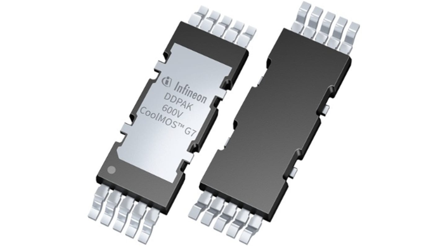
This image is representative of the product range
Bulk discount available
View bulk pricing optionsSubtotal (1 pack of 2 units)*
PHP711.40
(exc. VAT)
PHP796.76
(inc. VAT)
FREE delivery for orders over ₱3,000.00
In Stock
- 1,700 unit(s) ready to ship from another location
Need more? Click ‘Check delivery dates’ to find extra stock and lead times.
Units | Per Unit | Per Pack* |
|---|---|---|
| 2 - 8 | PHP355.70 | PHP711.40 |
| 10 - 98 | PHP325.84 | PHP651.68 |
| 100 - 248 | PHP301.22 | PHP602.44 |
| 250 - 498 | PHP279.215 | PHP558.43 |
| 500 + | PHP271.89 | PHP543.78 |
*price indicative
- RS Stock No.:
- 220-7418
- Mfr. Part No.:
- IPDD60R080G7XTMA1
- Manufacturer:
- Infineon
Specifications
Technical data sheets
Legislation and Compliance
Product Details
Find similar products by selecting one or more attributes.
Select all | Attribute | Value |
|---|---|---|
| Brand | Infineon | |
| Channel Type | Type N | |
| Product Type | MOSFET & Diode | |
| Maximum Continuous Drain Current Id | 83A | |
| Maximum Drain Source Voltage Vds | 650V | |
| Package Type | HDSOP | |
| Series | C7 GOLD | |
| Mount Type | Surface | |
| Pin Count | 10 | |
| Maximum Drain Source Resistance Rds | 80mΩ | |
| Channel Mode | Enhancement | |
| Maximum Power Dissipation Pd | 174W | |
| Typical Gate Charge Qg @ Vgs | 42nC | |
| Forward Voltage Vf | 0.8V | |
| Standards/Approvals | No | |
| Height | 21.11mm | |
| Length | 6.6mm | |
| Automotive Standard | No | |
| Select all | ||
|---|---|---|
Brand Infineon | ||
Channel Type Type N | ||
Product Type MOSFET & Diode | ||
Maximum Continuous Drain Current Id 83A | ||
Maximum Drain Source Voltage Vds 650V | ||
Package Type HDSOP | ||
Series C7 GOLD | ||
Mount Type Surface | ||
Pin Count 10 | ||
Maximum Drain Source Resistance Rds 80mΩ | ||
Channel Mode Enhancement | ||
Maximum Power Dissipation Pd 174W | ||
Typical Gate Charge Qg @ Vgs 42nC | ||
Forward Voltage Vf 0.8V | ||
Standards/Approvals No | ||
Height 21.11mm | ||
Length 6.6mm | ||
Automotive Standard No | ||
The Infineon technologies introduces Double DPAK (DDPAK), the first top-side cooled surface mount device (SMD) package addressing high power SMPS applications such as PC power, solar, server and telecom. The benefits of the already existing high voltage technology 600V Cool MOS G7 super junction (SJ) MOSFETis combined with the innovative concept of top-side cooling, providing a system solution for high current hard switching topologies such as PFC and a high-end efficiency solution for LLC topologies.
Gives best-in-class FOM RDS(on) x Eoss and RDS(on) x Qg
Innovative top-side cooling concept
Inbuilt 4th pin Kelvin source configuration and low parasitic source inductance
TCOB capability of >> 2.000 cycles, MSL1 compliant and total Pb-free
Enabling highest energy efficiency
Thermal decoupling of board and semiconductor allows to overcome thermal PCB limits
Reduced parasitic source inductance improves e efficiency and ease-of-use
Enables higher power density solutions
Exceeding the highest quality standards
Related links
- Infineon C7 GOLD Type N-Channel MOSFET & Diode 650 V Enhancement, 10-Pin HDSOP
- Infineon C7 GOLD Type N-Channel MOSFET & Diode 650 V Enhancement, 10-Pin HDSOP
- Infineon C7 GOLD Type N-Channel MOSFET & Diode 650 V Enhancement, 10-Pin HDSOP IPDD60R150G7XTMA1
- Infineon C7 GOLD Type N-Channel MOSFET 650 V Enhancement, 8-Pin HSOF
- Infineon C7 GOLD Type N-Channel MOSFET 650 V Enhancement, 8-Pin HSOF IPT60R150G7XTMA1
- Infineon OptiMOS Type N-Channel MOSFET 650 V Enhancement, 10-Pin PG-HDSOP-10-1 IPDD60R050G7XTMA1
- Infineon OptiMOS Type N-Channel MOSFET 650 V Enhancement, 10-Pin PG-HDSOP-10 IPDD60R037CM8XTMA1
- Infineon OptiMOS Type N-Channel MOSFET 650 V Enhancement, 10-Pin PG-HDSOP-10 IPDD60R180CM8XTMA1