Lattice FPGA iCE40 LP/HX 1280 Cells, 64 kB 160 Blocks, 49-Pin UCBGA
- RS Stock No.:
- 168-4224
- Mfr. Part No.:
- ICE40LP1K-CM49
- Manufacturer:
- Lattice Semiconductor

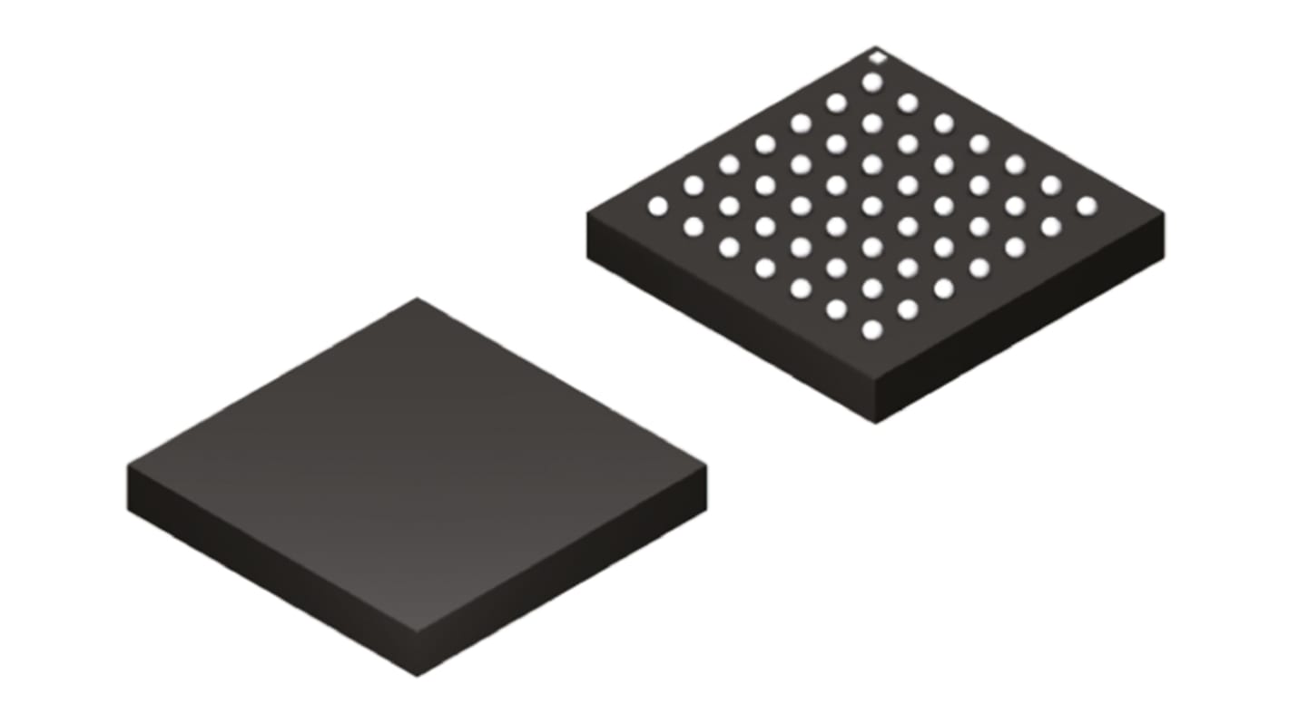
This image is representative of the product range
Currently unavailable
We don't know if this item will be back in stock, RS intend to remove it from our range soon.
- RS Stock No.:
- 168-4224
- Mfr. Part No.:
- ICE40LP1K-CM49
- Manufacturer:
- Lattice Semiconductor
Specifications
Technical data sheets
Legislation and Compliance
Product Details
Find similar products by selecting one or more attributes.
Select all | Attribute | Value |
|---|---|---|
| Brand | Lattice Semiconductor | |
| Series | iCE40 LP/HX | |
| Product Type | FPGA | |
| Number of Logic Cells | 1280 | |
| Number of Logic Units | 160 | |
| Number of Registers | 1280 | |
| Mount Type | Surface | |
| Minimum Supply Voltage | 1.14V | |
| Package Type | UCBGA | |
| Maximum Supply Voltage | 1.26V | |
| Pin Count | 49 | |
| Minimum Operating Temperature | -40°C | |
| Number of I/Os | 206 | |
| Number of RAM Bits | 64kB | |
| Maximum Operating Temperature | 85°C | |
| Height | 0.9mm | |
| Length | 3mm | |
| Standards/Approvals | Halogen Free | |
| Width | 3 mm | |
| Automotive Standard | No | |
| Select all | ||
|---|---|---|
Brand Lattice Semiconductor | ||
Series iCE40 LP/HX | ||
Product Type FPGA | ||
Number of Logic Cells 1280 | ||
Number of Logic Units 160 | ||
Number of Registers 1280 | ||
Mount Type Surface | ||
Minimum Supply Voltage 1.14V | ||
Package Type UCBGA | ||
Maximum Supply Voltage 1.26V | ||
Pin Count 49 | ||
Minimum Operating Temperature -40°C | ||
Number of I/Os 206 | ||
Number of RAM Bits 64kB | ||
Maximum Operating Temperature 85°C | ||
Height 0.9mm | ||
Length 3mm | ||
Standards/Approvals Halogen Free | ||
Width 3 mm | ||
Automotive Standard No | ||
- COO (Country of Origin):
- KR
Field Programmable Gate Arrays, Lattice Semiconductor
An FPGA is a semiconductor device consisting of a Matrix of Configurable Logic Blocks (CLBs) connected through programmable interconnects. The user determines these interconnections by programming SRAM. A CLB can be simple (AND, OR gates, etc) or complex (a Block of RAM). The FPGA allows changes to be MADE to a design even after the device is soldered into a PCB.
Related links
- Lattice FPGA ICE40HX1K-VQ100 64kbit 100-Pin VQFP
- Lattice FPGA ICE40HX4K-TQ144 80kbit 144-Pin TQFP
- Lattice Semiconductor Complex Programmable Logic Device ispMACH EEPROM 32 Cells 7.5 ns 36 Labs, In System
- Lattice Semiconductor Complex Programmable Logic Device ispMACH EEPROM 64 Cells 7.5 ns 36 Labs, In System
- Lattice Semiconductor Complex Programmable Logic Device ispMACH EEPROM 128 Cells 7.5 ns 36 Labs, In System
- Lattice Semiconductor Complex Programmable Logic Device ispMACH EEPROM 32 Cells 7.5 ns 2 Labs, In System
- Lattice Semiconductor Complex Programmable Logic Device ispMACH EEPROM 256 Cells 7.5 ns 36 Labs, In System
- Lattice Semiconductor Complex Programmable Logic Device ispMACH EEPROM 64 Cells 7.5 ns 36 Labs, In System