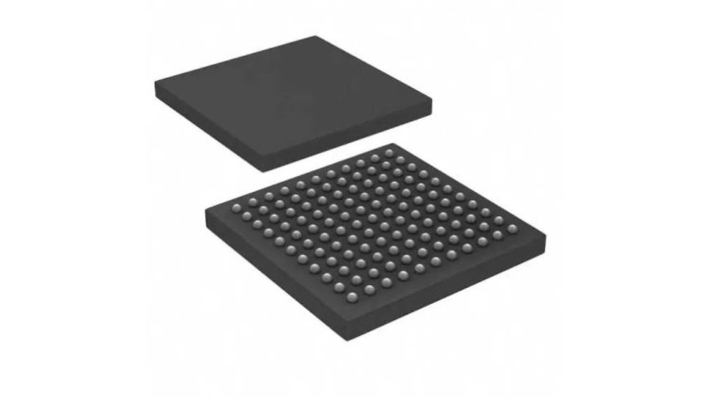
Infineon NOR 128 MB CFI, SPI Flash Memory 8-Pin WSON, S25FL128SAGNFV000
- RS Stock No.:
- 181-8392
- Mfr. Part No.:
- S25FL128SAGNFV000
- Manufacturer:
- Infineon

Bulk discount available
View bulk pricing optionsSubtotal (1 pack of 3 units)*
PHP944.799
(exc. VAT)
PHP1,058.175
(inc. VAT)
FREE delivery for orders over ₱3,000.00
In Stock
- 270 unit(s) ready to ship from another location
Need more? Click ‘Check delivery dates’ to find extra stock and lead times.
Units | Per Unit | Per Pack* |
|---|---|---|
| 3 - 27 | PHP314.933 | PHP944.80 |
| 30 - 72 | PHP295.277 | PHP885.83 |
| 75 - 147 | PHP281.973 | PHP845.92 |
| 150 - 297 | PHP279.023 | PHP837.07 |
| 300 + | PHP259.00 | PHP777.00 |
*price indicative
- RS Stock No.:
- 181-8392
- Mfr. Part No.:
- S25FL128SAGNFV000
- Manufacturer:
- Infineon
Specifications
Technical data sheets
Legislation and Compliance
Product Details
Find similar products by selecting one or more attributes.
Select all | Attribute | Value |
|---|---|---|
| Brand | Infineon | |
| Product Type | Flash Memory | |
| Memory Size | 128MB | |
| Interface Type | CFI, SPI | |
| Package Type | WSON | |
| Pin Count | 8 | |
| Organisation | 16M x 8 bit | |
| Mount Type | Surface | |
| Maximum Clock Frequency | 133MHz | |
| Cell Type | NOR | |
| Minimum Supply Voltage | 1.65V | |
| Maximum Supply Voltage | 3.6V | |
| Minimum Operating Temperature | -40°C | |
| Maximum Operating Temperature | 105°C | |
| Height | 0.75mm | |
| Length | 6mm | |
| Width | 8mm | |
| Standards/Approvals | No | |
| Number of Banks | 2 | |
| Maximum Random Access Time | 14.5ns | |
| Automotive Standard | AEC-Q100 | |
| Series | S25FL128S | |
| Number of Words | 16M | |
| Number of Bits per Word | 8 | |
| Select all | ||
|---|---|---|
Brand Infineon | ||
Product Type Flash Memory | ||
Memory Size 128MB | ||
Interface Type CFI, SPI | ||
Package Type WSON | ||
Pin Count 8 | ||
Organisation 16M x 8 bit | ||
Mount Type Surface | ||
Maximum Clock Frequency 133MHz | ||
Cell Type NOR | ||
Minimum Supply Voltage 1.65V | ||
Maximum Supply Voltage 3.6V | ||
Minimum Operating Temperature -40°C | ||
Maximum Operating Temperature 105°C | ||
Height 0.75mm | ||
Length 6mm | ||
Width 8mm | ||
Standards/Approvals No | ||
Number of Banks 2 | ||
Maximum Random Access Time 14.5ns | ||
Automotive Standard AEC-Q100 | ||
Series S25FL128S | ||
Number of Words 16M | ||
Number of Bits per Word 8 | ||
This family of devices connect to a host system via a SPI. Traditional SPI single bit serial input and output (Single I/O or SIO) is
supported as well as optional two bit (Dual I/O or DIO) and four bit (Quad I/O or QIO) serial commands. This multiple width interface
is called SPI Multi-I/O or MIO. In addition, the FL-S family adds support for DDR read commands for SIO, DIO, and QIO that transfer
address and read data on both edges of the clock.
The Eclipse architecture features a Page Programming Buffer that allows up to 128 words (256 bytes) or 256 words (512 bytes) to be
programmed in one operation, resulting in faster effective programming and erase than prior generation SPI program or erase
algorithms.
Executing code directly from flash memory is often called Execute-In-Place or XIP. By using FL-S devices at the higher clock rates
supported, with QIO or DDR-QIO commands, the instruction read transfer rate can match or exceed traditional parallel interface,
asynchronous, NOR flash memories while reducing signal count dramatically.
The S25FL128S and S25FL256S products offer high densities coupled with the flexibility and fast performance required by a variety
of embedded applications. They are ideal for code shadowing, XIP, and data storage.
Related links
- Infineon NOR 128 MB CFI, SPI Flash Memory 8-Pin WSON
- Winbond NOR 128 MB Quad-SPI Flash Memory 8-Pin WSON
- Infineon NOR 128 MB Quad-SPI Flash Memory 8-Pin WSON
- Infineon NOR 128 MB SPI Flash Memory 8-Pin WSON
- Infineon NOR 128 MB Quad-SPI Flash Memory 8-Pin WSON, S25FL128LAGNFI010
- Infineon NOR 128 MB SPI Flash Memory 8-Pin WSON, S25FL128LAGNFV010
- Winbond NOR 128 MB Quad-SPI Flash Memory 8-Pin WSON, W25Q128JVEIM
- Winbond NOR 128 MB SPI Flash Memory 8-Pin WSON