Renesas Electronics 5PB1102PGGI Clock Buffer, 14-Pin 2 TSSOP
- RS Stock No.:
- 216-6167
- Mfr. Part No.:
- 5PB1102PGGI
- Manufacturer:
- Renesas Electronics

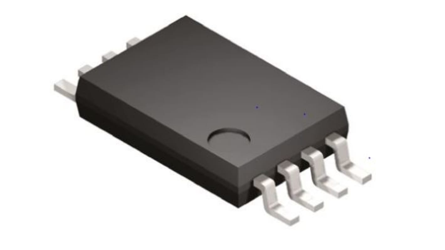
This image is representative of the product range
Bulk discount available
View bulk pricing optionsSubtotal (1 pack of 5 units)*
PHP565.25
(exc. VAT)
PHP633.10
(inc. VAT)
FREE delivery for orders over ₱3,000.00
In Stock
- Plus 470 unit(s) shipping from July 20, 2026
Need more? Click ‘Check delivery dates’ to find extra stock and lead times.
Units | Per Unit | Per Pack* |
|---|---|---|
| 5 - 5 | PHP113.05 | PHP565.25 |
| 10 - 20 | PHP95.954 | PHP479.77 |
| 25 - 45 | PHP94.042 | PHP470.21 |
| 50 - 95 | PHP92.13 | PHP460.65 |
| 100 + | PHP82.176 | PHP410.88 |
*price indicative
- RS Stock No.:
- 216-6167
- Mfr. Part No.:
- 5PB1102PGGI
- Manufacturer:
- Renesas Electronics
Specifications
Technical data sheets
Legislation and Compliance
Product Details
Find similar products by selecting one or more attributes.
Select all | Attribute | Value |
|---|---|---|
| Brand | Renesas Electronics | |
| Product Type | Clock Buffer | |
| Mount Type | Surface | |
| Package Type | TSSOP | |
| Pin Count | 14 | |
| Minimum Supply Voltage | 1.8V | |
| Maximum Supply Voltage | 3.3V | |
| Minimum Operating Temperature | -40°C | |
| Maximum Operating Temperature | 105°C | |
| Standards/Approvals | No | |
| Series | 5PB1102 | |
| Length | 3.1mm | |
| Height | 1mm | |
| Maximum Output Frequency | 200MHz | |
| Automotive Standard | No | |
| Select all | ||
|---|---|---|
Brand Renesas Electronics | ||
Product Type Clock Buffer | ||
Mount Type Surface | ||
Package Type TSSOP | ||
Pin Count 14 | ||
Minimum Supply Voltage 1.8V | ||
Maximum Supply Voltage 3.3V | ||
Minimum Operating Temperature -40°C | ||
Maximum Operating Temperature 105°C | ||
Standards/Approvals No | ||
Series 5PB1102 | ||
Length 3.1mm | ||
Height 1mm | ||
Maximum Output Frequency 200MHz | ||
Automotive Standard No | ||
The Renesas Electronics 5PB11xx is a high-performance LVCMOS clock buffer family of devices. It has an additive phase jitter of 50fs RMS. There are five different fan-out variations available: 1:2 to 1:10. The 5PB11xx supports a synchronous glitch-free output enable (OE) function to eliminate any potential intermediate incorrect output clock cycles when enabling or disabling outputs. It can operate from a 1.8V to 3.3V supply.
High-performance 1:2, 1:4, 1:6, 1:8, 1:10 LVCMOS clock buffer
Very low pin-to-pin skew: < 50ps
Very low additive jitter: < 50fs
Supply voltage: 1.8V to 3.3V
3.3V tolerant input clock
fMAX = 200MHz
Integrated serial termination for 50Ω channel
Related links
- Renesas Electronics 5PB1102PGGI Clock Buffer, 14-Pin 2 TSSOP
- Renesas Electronics 5PB1106PGGI Clock Buffer, 14-Pin 6 TSSOP
- Renesas Electronics 557GI-03LF Clock Generator, 16-Pin 2 TSSOP
- Renesas Electronics 8305AGILF Clock Buffer, 16-Pin 4 TSSOP
- Renesas Electronics 8305AGLF Clock Buffer, 16-Pin 4 TSSOP
- Renesas Electronics 5PB1102CMGI8 Clock Buffer, 8-Pin TSSOP
- Renesas Electronics 5PB1104PGGI Clock Buffer, 8-Pin 4 TSSOP
- Renesas Electronics 85102AGILF Clock Buffer, 16-Pin 7 TSSOP