Toshiba 74VHCT541AFT 3 State Octal Bus Buffer, 20-Pin TSSOP
- RS Stock No.:
- 171-3523
- Mfr. Part No.:
- 74VHCT541AFT
- Manufacturer:
- Toshiba

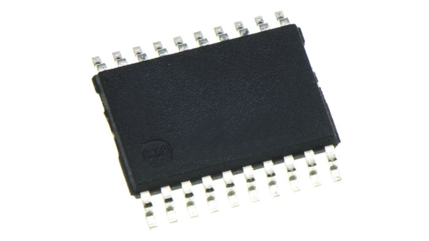
This image is representative of the product range
Bulk discount available
View bulk pricing optionsSubtotal (1 pack of 25 units)*
PHP388.50
(exc. VAT)
PHP435.00
(inc. VAT)
FREE delivery for orders over ₱3,000.00
In Stock
- Plus 325 unit(s) shipping from July 20, 2026
- Plus 7,950 unit(s) shipping from July 27, 2026
Need more? Click ‘Check delivery dates’ to find extra stock and lead times.
Units | Per Unit | Per Pack* |
|---|---|---|
| 25 - 75 | PHP15.54 | PHP388.50 |
| 100 - 475 | PHP15.074 | PHP376.85 |
| 500 - 975 | PHP14.622 | PHP365.55 |
| 1000 + | PHP14.183 | PHP354.58 |
*price indicative
- RS Stock No.:
- 171-3523
- Mfr. Part No.:
- 74VHCT541AFT
- Manufacturer:
- Toshiba
Specifications
Technical data sheets
Legislation and Compliance
Product Details
Find similar products by selecting one or more attributes.
Select all | Attribute | Value |
|---|---|---|
| Brand | Toshiba | |
| Product Type | Octal Bus Buffer | |
| Logic Family | 74VHCT | |
| Logic Function | Buffer | |
| Schmitt Trigger Input | No | |
| Input Type | CMOS | |
| Output Type | 3 State | |
| Mount Type | Surface | |
| Minimum Supply Voltage | 4.5V | |
| Package Type | TSSOP | |
| Pin Count | 20 | |
| Maximum Supply Voltage | 5.5V | |
| Maximum Propagation Delay Time @ CL | 5.4ns | |
| Maximum High Level Output Current | -8mA | |
| Minimum Operating Temperature | -40°C | |
| Maximum Low Level Output Current | 8mA | |
| Maximum Operating Temperature | 125°C | |
| Length | 6.5mm | |
| Series | 74VHC | |
| Standards/Approvals | No | |
| Height | 1mm | |
| Supply Current | 4μA | |
| Automotive Standard | AEC-Q100 | |
| Select all | ||
|---|---|---|
Brand Toshiba | ||
Product Type Octal Bus Buffer | ||
Logic Family 74VHCT | ||
Logic Function Buffer | ||
Schmitt Trigger Input No | ||
Input Type CMOS | ||
Output Type 3 State | ||
Mount Type Surface | ||
Minimum Supply Voltage 4.5V | ||
Package Type TSSOP | ||
Pin Count 20 | ||
Maximum Supply Voltage 5.5V | ||
Maximum Propagation Delay Time @ CL 5.4ns | ||
Maximum High Level Output Current -8mA | ||
Minimum Operating Temperature -40°C | ||
Maximum Low Level Output Current 8mA | ||
Maximum Operating Temperature 125°C | ||
Length 6.5mm | ||
Series 74VHC | ||
Standards/Approvals No | ||
Height 1mm | ||
Supply Current 4μA | ||
Automotive Standard AEC-Q100 | ||
The 74VHCT540AFT and 74VHCT541AFT are Advanced high speed CMOS OCTAL BUS BUFFERs fabricated with silicon gate C2MOS technology. They achieve the high speed operation similar to equivalent Bipolar Schottky TTL while maintaining the CMOS low power dissipation. The 74VHCT240AFT is an inverting 3-state buffer having two active-low output enables. The 74VHCT244AFT is a non-inverting 3-state buffer, and has two active-low output enables. These devices are designed to be used with 3-state memory address drivers, etc. The input voltage are compatible with TTL output voltage. These devices may be used as a level converter for interfacing 3.3 V to 5 V system. Input protection and output circuit ensure that 0 to 5.5 V can be applied to the input and output (Note) pins without regard to the supply voltage. These structure prevents device destruction due to mismatched supply and input/output voltages such as battery back up, hot board insertion, etc
Wide operating temperature range: Topr = -40 to 125
High speed: tpd = 5.4 ns (typ.) at VCC = 5.0 V
Low power dissipation: ICC = 2.0 μA (max) at Ta = 25
Compatible with TTL inputs : VIL = 0.8 V (max): VIH = 2.0 V (min)
Power down protection is provided on all inputs and outputs.
Balanced propagation delays: tPLH ≈ tPHL
Low noise: VOLP = 1.0 V (max)
Pin and function compatible with the 74 series (AC/HC/AHC/LV etc.) 245 type
Related links
- Toshiba 3 State Octal Bus Buffer, 20-Pin TSSOP
- Toshiba 74VHC540FT 3 State Octal Bus Buffer, 20-Pin TSSOP
- Toshiba Schmitt Trigger Input 3 State Octal Bus Buffer, 20-Pin TSSOP
- Toshiba 74VHCV541FT Schmitt Trigger Input 3 State Octal Bus Buffer, 20-Pin TSSOP
- Toshiba 74HC244D Non-Inverting 3 State Octal Bus Buffer, 20-Pin SOIC
- Toshiba Non-Inverting 3 State Octal Bus Buffer, 20-Pin SOIC
- Toshiba Non-Inverting 3 State Octal Bus Buffer, 14-Pin TSSOP
- Toshiba 74VHCT126AFT Non-Inverting 3 State Octal Bus Buffer, 14-Pin TSSOP