onsemi PowerTrench Type P-Channel MOSFET, 11 A, 30 V Enhancement, 8-Pin SOIC
- RS Stock No.:
- 166-2610
- Mfr. Part No.:
- FDS6675BZ
- Manufacturer:
- onsemi

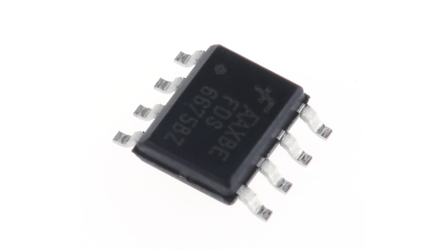
This image is representative of the product range
Supply shortage
Due to a global supply shortage, we don't know when this will be back in stock.
- RS Stock No.:
- 166-2610
- Mfr. Part No.:
- FDS6675BZ
- Manufacturer:
- onsemi
Specifications
Technical data sheets
Legislation and Compliance
Product Details
Find similar products by selecting one or more attributes.
Select all | Attribute | Value |
|---|---|---|
| Brand | onsemi | |
| Channel Type | Type P | |
| Product Type | MOSFET | |
| Maximum Continuous Drain Current Id | 11A | |
| Maximum Drain Source Voltage Vds | 30V | |
| Series | PowerTrench | |
| Package Type | SOIC | |
| Mount Type | Surface | |
| Pin Count | 8 | |
| Maximum Drain Source Resistance Rds | 13mΩ | |
| Channel Mode | Enhancement | |
| Forward Voltage Vf | -1.2V | |
| Typical Gate Charge Qg @ Vgs | 44nC | |
| Maximum Power Dissipation Pd | 2.5W | |
| Minimum Operating Temperature | -55°C | |
| Maximum Operating Temperature | 150°C | |
| Length | 5mm | |
| Standards/Approvals | No | |
| Height | 1.5mm | |
| Automotive Standard | No | |
| Select all | ||
|---|---|---|
Brand onsemi | ||
Channel Type Type P | ||
Product Type MOSFET | ||
Maximum Continuous Drain Current Id 11A | ||
Maximum Drain Source Voltage Vds 30V | ||
Series PowerTrench | ||
Package Type SOIC | ||
Mount Type Surface | ||
Pin Count 8 | ||
Maximum Drain Source Resistance Rds 13mΩ | ||
Channel Mode Enhancement | ||
Forward Voltage Vf -1.2V | ||
Typical Gate Charge Qg @ Vgs 44nC | ||
Maximum Power Dissipation Pd 2.5W | ||
Minimum Operating Temperature -55°C | ||
Maximum Operating Temperature 150°C | ||
Length 5mm | ||
Standards/Approvals No | ||
Height 1.5mm | ||
Automotive Standard No | ||
PowerTrench® P-Channel MOSFET, Fairchild Semiconductor
PowerTrench® MOSFETs are optimised power switches that offer increase of system efficiency and power density. They combine small gate charge(Qg), small reverse recovery charge(Qrr) and soft reverse recovery body diode, which contributes to fast switching of synchronous rectification in AC/DC power supplies.
The latest PowerTrench® MOSFETs employa shielded-gate structure that provides charge balance. By utilizing this Advanced technology, the FOM (Figure of Merit) of these devices is significant lower than that of previous generations.
Soft body diode performance of the PowerTrench® MOSFETs is able to eliminate snubber circuits or replace a higher voltage rating MOSFET.
MOSFET Transistors, ON Semi
ON Semi offers a substantial portfolio of MOSFET devices that includes high-voltage (>250V) and low-voltage (<250V) types. The Advanced silicon technology provides smaller die sizes, which it is incorporated into multiple industry-standard and thermally-enhanced packages.
ON Semi MOSFETs provide superior design reliability from reduced voltage spikes and overshoot, to lower junction capacitance and reverse recovery charge, to elimination of additional external components to keep systems up and running longer.
Related links
- onsemi PowerTrench Type P-Channel MOSFET 30 V Enhancement, 8-Pin SOIC FDS6675BZ
- onsemi PowerTrench Type P-Channel MOSFET 20 V Enhancement, 8-Pin SOIC
- onsemi PowerTrench Type P-Channel MOSFET 20 V Enhancement, 8-Pin SOIC FDS6576
- onsemi PowerTrench Type P-Channel MOSFET 30 V Enhancement, 3-Pin TO-252
- onsemi PowerTrench Type P-Channel MOSFET 30 V Enhancement, 3-Pin TO-252 FDD6685
- onsemi PowerTrench Type P-Channel MOSFET 30 V Enhancement, 8-Pin SOIC
- onsemi PowerTrench Type P-Channel MOSFET 40 V Enhancement, 8-Pin SOIC
- onsemi PowerTrench Type P-Channel MOSFET 30 V Enhancement, 8-Pin SOIC