Digilent 410-183 Basys Artix-7 Development Board ADC1410 for DAC121S101
- RS Stock No.:
- 134-6451
- Distrelec Article No.:
- 300-44-247
- Mfr. Part No.:
- 410-183
- Manufacturer:
- Digilent

Subtotal (1 unit)*
PHP13,013.89
(exc. VAT)
PHP14,575.56
(inc. VAT)
FREE delivery for orders over ₱3,000.00
In Stock
- 56 unit(s) ready to ship from another location
- Plus 30 unit(s) shipping from July 24, 2026
- Plus 2 unit(s) shipping from July 24, 2026
Need more? Click ‘Check delivery dates’ to find extra stock and lead times.
Units | Per Unit |
|---|---|
| 1 + | PHP13,013.89 |
*price indicative
- RS Stock No.:
- 134-6451
- Distrelec Article No.:
- 300-44-247
- Mfr. Part No.:
- 410-183
- Manufacturer:
- Digilent
Specifications
Technical data sheets
Legislation and Compliance
Product Details
Find similar products by selecting one or more attributes.
Select all | Attribute | Value |
|---|---|---|
| Brand | Digilent | |
| Programmable Logic Technology | FPGA | |
| Kit Classification | Development Board | |
| Product Type | Programmable Logic Development Kit | |
| For Use With | DAC121S101 | |
| Featured Device | ADC1410 | |
| Kit Name | Basys Artix-7 | |
| Standards/Approvals | RoHS | |
| Select all | ||
|---|---|---|
Brand Digilent | ||
Programmable Logic Technology FPGA | ||
Kit Classification Development Board | ||
Product Type Programmable Logic Development Kit | ||
For Use With DAC121S101 | ||
Featured Device ADC1410 | ||
Kit Name Basys Artix-7 | ||
Standards/Approvals RoHS | ||
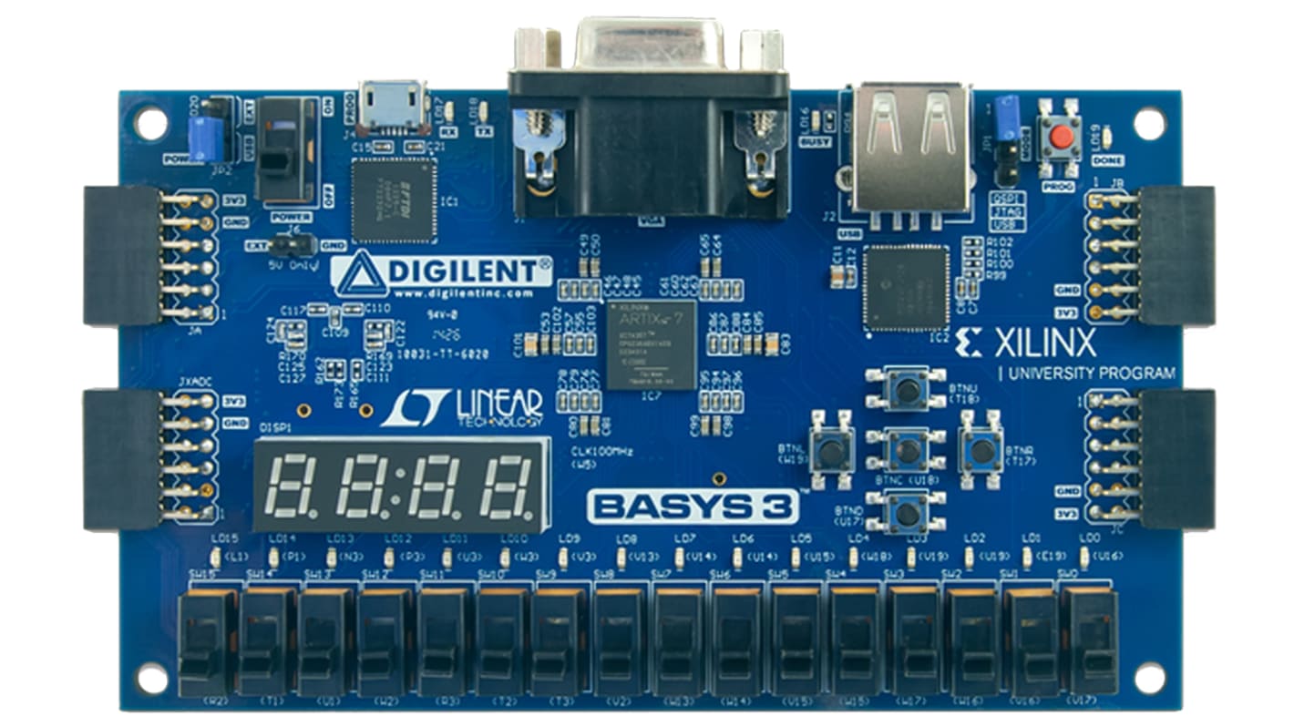
Digilent BASYS 3™ FQGA Development Board
The Digilent basys 3™ FPGA development board is a comprehensive, ready-to-use digital circuit development platform based on the latest Artix-7 Field Programmable Gate Array (FPGA) from Xilinx. With high-capacity FPGA, low overall cost and collection of USB, VGA and other ports, the board can host designs ranging from introductory combinational circuits to complex sequential circuits like embedded processors and controllers. It includes enough switches, LEDs and other I/O devices to allow a large number of designs to be completed without the need for any additional hardware and enough uncommitted FPGA I/O pins to allow designs to be expanded using diligent Pmods or other custom boards and circuits.
An FPGA is a semiconductor device consisting of a matrix of Configurable Logic Blocks (CLBs) connected through programmable interconnects. The user determines these interconnections by programming SRAM. A CLB can be simple (AND, OR gates, etc) or complex (a block of RAM). The FPGA allows changes to be made to design even after the device is soldered into a PC
Features and Benefits
33280 logic cells in 5200 slices (each slice contains 4 x 6-input LUTs and 8 x flip-flops)
1800Kbit fast block RAM
5 x clock management tiles, each with a phase-locked loop (PLL)
90 x DSP slices
Internal clock speeds exceeding 450MHz
On-chip analogue to digital converter (XADC)
Onboard 32Mbit Quad-SPI serial flash memory
Programmable over JTAG, Quad-SPI or USB
USB-UART Bridge via microUSB socket
USB-A HID host socket for mice, keyboards and memory sticks
12-bit VGA display output on DE15 connector
FPGA programming
16 x user LEDs
4-digit 7-segment LED display
5 x user pushbuttons
16 x user slide switches
3 x standard Pmod 2 x 6-pin connectors
Dual purpose
Powered from either USB socket or external 5V header
Certifications
ANSI/ESD S20.20:2014
BS EN 61340-5-1:2007
Related links
- Digilent 410-316 Nexys Video Artix-7 Development Board ADC1410 for DAC121S101
- Digilent 410-292 Nexys A7-100T Nexys 4 DDR Artix-7 Development Board ADC1410 for DAC121S101
- Digilent 410-300 GENESYS2 KINTEX-7 Development Board ADC1410 for DAC121S101
- Digilent 410-328-35 Cmod A7 Artix-7 Module ADC1410 for DAC121S101
- Digilent 410-319-1 FPGA Development Board for Makers and Hobbyists Development Board ADC1410 for DAC121S101
- Digilent 410-376 Xilinx Spartan-7 Development Board ADC1410 for XC7S25 Spartan-7
- Digilent 410-352 Xilinx Spartan-7 Development Board ADC1410 for Hobbyists Makers
- Digilent 410-370 Cora Z7: Zynq-7000 Development Board ADC1410 for FPGA Development, ARM Development