Renesas Electronics 8305AGILF Clock Buffer, 16-Pin 4 TSSOP
- RS Stock No.:
- 216-6204
- Mfr. Part No.:
- 8305AGILF
- Manufacturer:
- Renesas Electronics

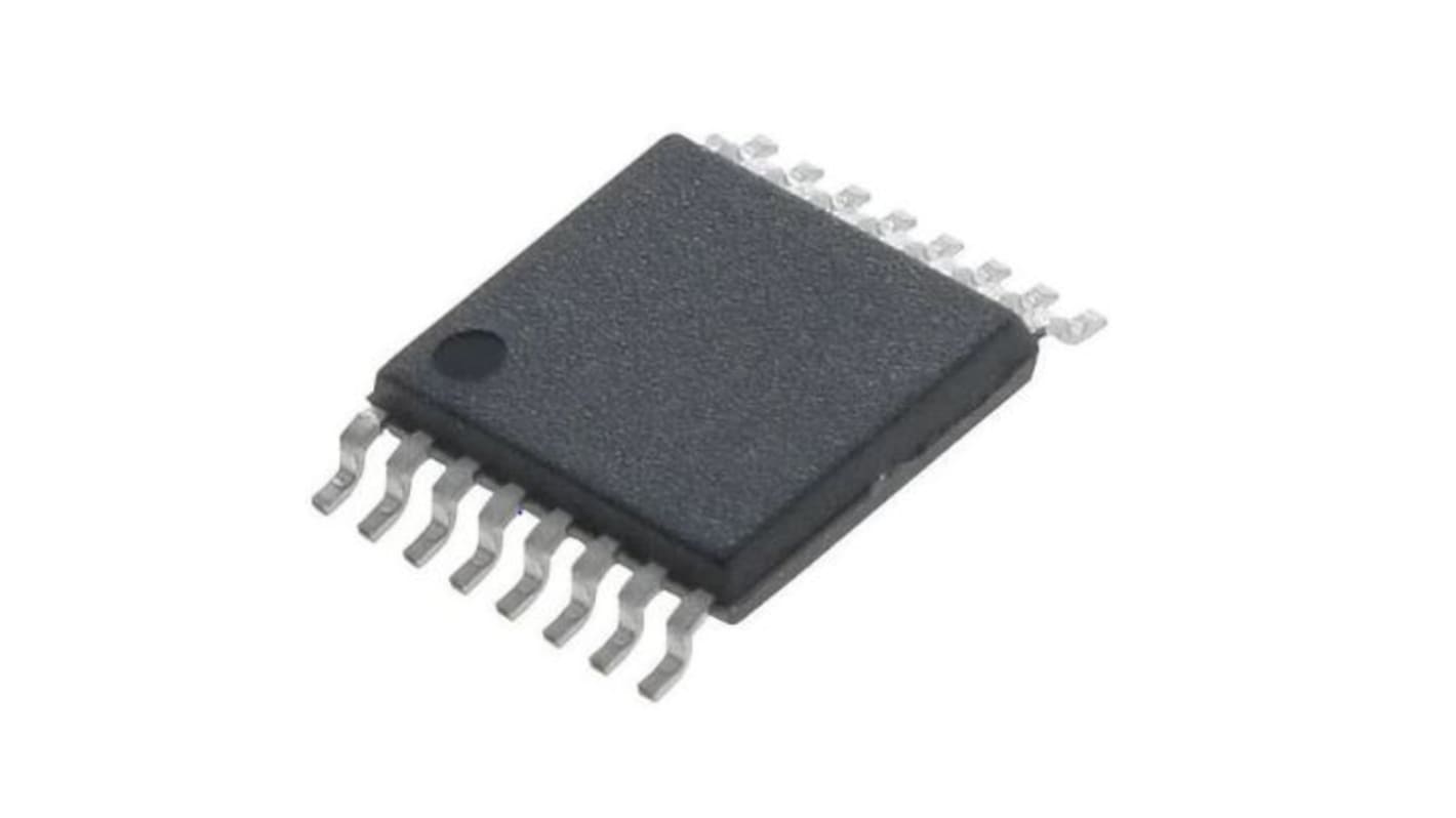
This image is representative of the product range
Currently unavailable
We don't know if this item will be back in stock, RS intend to remove it from our range soon.
- RS Stock No.:
- 216-6204
- Mfr. Part No.:
- 8305AGILF
- Manufacturer:
- Renesas Electronics
Specifications
Technical data sheets
Legislation and Compliance
Product Details
Find similar products by selecting one or more attributes.
Select all | Attribute | Value |
|---|---|---|
| Brand | Renesas Electronics | |
| Product Type | Clock Buffer | |
| Mount Type | Surface | |
| Package Type | TSSOP | |
| Minimum Supply Voltage | 1.8V | |
| Pin Count | 16 | |
| Maximum Supply Voltage | 3.3V | |
| Minimum Operating Temperature | -40°C | |
| Maximum Operating Temperature | 85°C | |
| Length | 4.9mm | |
| Height | 1.2mm | |
| Standards/Approvals | No | |
| Series | 8305A | |
| Automotive Standard | No | |
| Select all | ||
|---|---|---|
Brand Renesas Electronics | ||
Product Type Clock Buffer | ||
Mount Type Surface | ||
Package Type TSSOP | ||
Minimum Supply Voltage 1.8V | ||
Pin Count 16 | ||
Maximum Supply Voltage 3.3V | ||
Minimum Operating Temperature -40°C | ||
Maximum Operating Temperature 85°C | ||
Length 4.9mm | ||
Height 1.2mm | ||
Standards/Approvals No | ||
Series 8305A | ||
Automotive Standard No | ||
The Renesas Electronics ICS8305I is a low skew, 1-to-4, Differential/LVCMOS-toLVCMOS/LVTTL Fanout Buffer. The ICS8305I has selectable clock inputs that accept either differential or single ended input levels. The clock enable is internally synchronized to eliminate runt pulses on the outputs during asynchronous assertion/deassertion of the clock enable pin. Outputs are forced LOW when the clock is disabled. A separate output enable pin controls whether the outputs are in the active or high impedance state.
4 LVCMOS/LVTTL outputs
Selectable differential or LVCMOS/LVTTL clock inputs
CLK, nCLK pair can accept the following differential
input levels: LVPECL, LVDS, LVHSTL, HCSL, SSTL
LVCMOS_CLK supports the following input types:
LVCMOS, LVTTL
Maximum output frequency: 350MHz
Output skew: 40ps (maximum)
Part-to-part skew: 700ps (maximum)
Additive phase jitter, RMS: 0.04ps (typical)
3.3V core, 3.3V, 2.5V or 1.8V output operating supply
-40°C to 85°C ambient operating temperature
Lead-Free package fully RoHS compliant
Related links
- Renesas Electronics 8305AGILF Clock Buffer, 16-Pin 4 TSSOP
- Renesas Electronics 8305AGLF Clock Buffer, 16-Pin 4 TSSOP
- Renesas Electronics 85102AGILF Clock Buffer, 16-Pin 7 TSSOP
- Renesas Electronics 5PB1106CMGI Clock Buffer, 16-Pin 4 VFQFPN
- Renesas Electronics 9DMV0141AKILF Clock Buffer, 16-Pin 1 VFQFPN
- Renesas Electronics 5PB1108PGGI Clock Buffer, 16-Pin 8 VFQFPN
- Renesas Electronics 5PB1108CMGI Clock Buffer, 16-Pin 8 VFQFPN
- Renesas Electronics 5PB1104PGGI Clock Buffer, 8-Pin 4 TSSOP