Renesas Electronics 2309-1HPGG Clock Buffer 16-Pin TSSOP
- RS Stock No.:
- 263-7880P
- Mfr. Part No.:
- 2309-1HPGG
- Manufacturer:
- Renesas Electronics

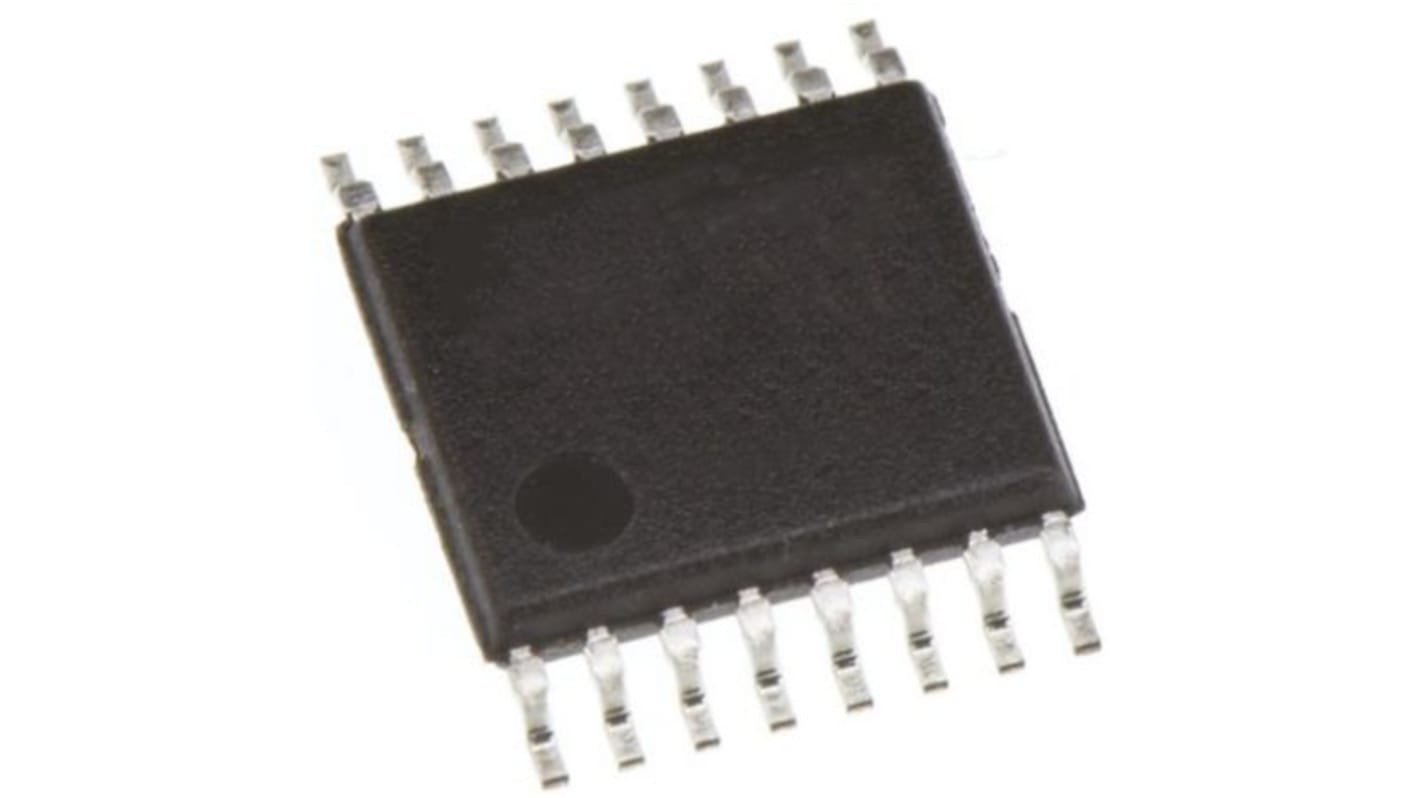
This image is representative of the product range
Bulk discount available
Subtotal 10 units (supplied in a tube)*
PHP772.92
(exc. VAT)
PHP865.67
(inc. VAT)
FREE delivery for orders over ₱3,000.00
In Stock
- 565 unit(s) ready to ship from another location
Need more? Click ‘Check delivery dates’ to find extra stock and lead times.
Units | Per Unit |
|---|---|
| 10 - 20 | PHP77.292 |
| 25 - 45 | PHP72.308 |
| 50 - 90 | PHP70.868 |
| 95 + | PHP69.428 |
*price indicative
- RS Stock No.:
- 263-7880P
- Mfr. Part No.:
- 2309-1HPGG
- Manufacturer:
- Renesas Electronics
Specifications
Technical data sheets
Legislation and Compliance
Product Details
Find similar products by selecting one or more attributes.
Select all | Attribute | Value |
|---|---|---|
| Brand | Renesas Electronics | |
| Product Type | Clock Buffer | |
| Maximum Input Frequency | 133MHz | |
| Mount Type | Surface | |
| Package Type | TSSOP | |
| Pin Count | 16 | |
| Number of Outputs | 15 | |
| Minimum Supply Voltage | -0.5V | |
| Maximum Supply Voltage | 4.6V | |
| Minimum Operating Temperature | 0°C | |
| Maximum Operating Temperature | 70°C | |
| Height | 1mm | |
| Standards/Approvals | RoHS | |
| Width | 4.4 mm | |
| Series | IDT2309 | |
| Length | 5mm | |
| Automotive Standard | No | |
| Select all | ||
|---|---|---|
Brand Renesas Electronics | ||
Product Type Clock Buffer | ||
Maximum Input Frequency 133MHz | ||
Mount Type Surface | ||
Package Type TSSOP | ||
Pin Count 16 | ||
Number of Outputs 15 | ||
Minimum Supply Voltage -0.5V | ||
Maximum Supply Voltage 4.6V | ||
Minimum Operating Temperature 0°C | ||
Maximum Operating Temperature 70°C | ||
Height 1mm | ||
Standards/Approvals RoHS | ||
Width 4.4 mm | ||
Series IDT2309 | ||
Length 5mm | ||
Automotive Standard No | ||
- COO (Country of Origin):
- PH
The Renesas Electronics high-speed phase-lock loop clock buffer, designed to address high-speed clock distribution applications. The zero delay is achieved by aligning the phase between the incoming clock and the output clock, operable within the range of 10 to 133MHz. It is an 8-pin version of the accepts one reference input, and drives out five low skew clocks.
Phase lock loop clock distribution
Distributes one clock input to one bank of five outputs
No external RC network required
Power down mode