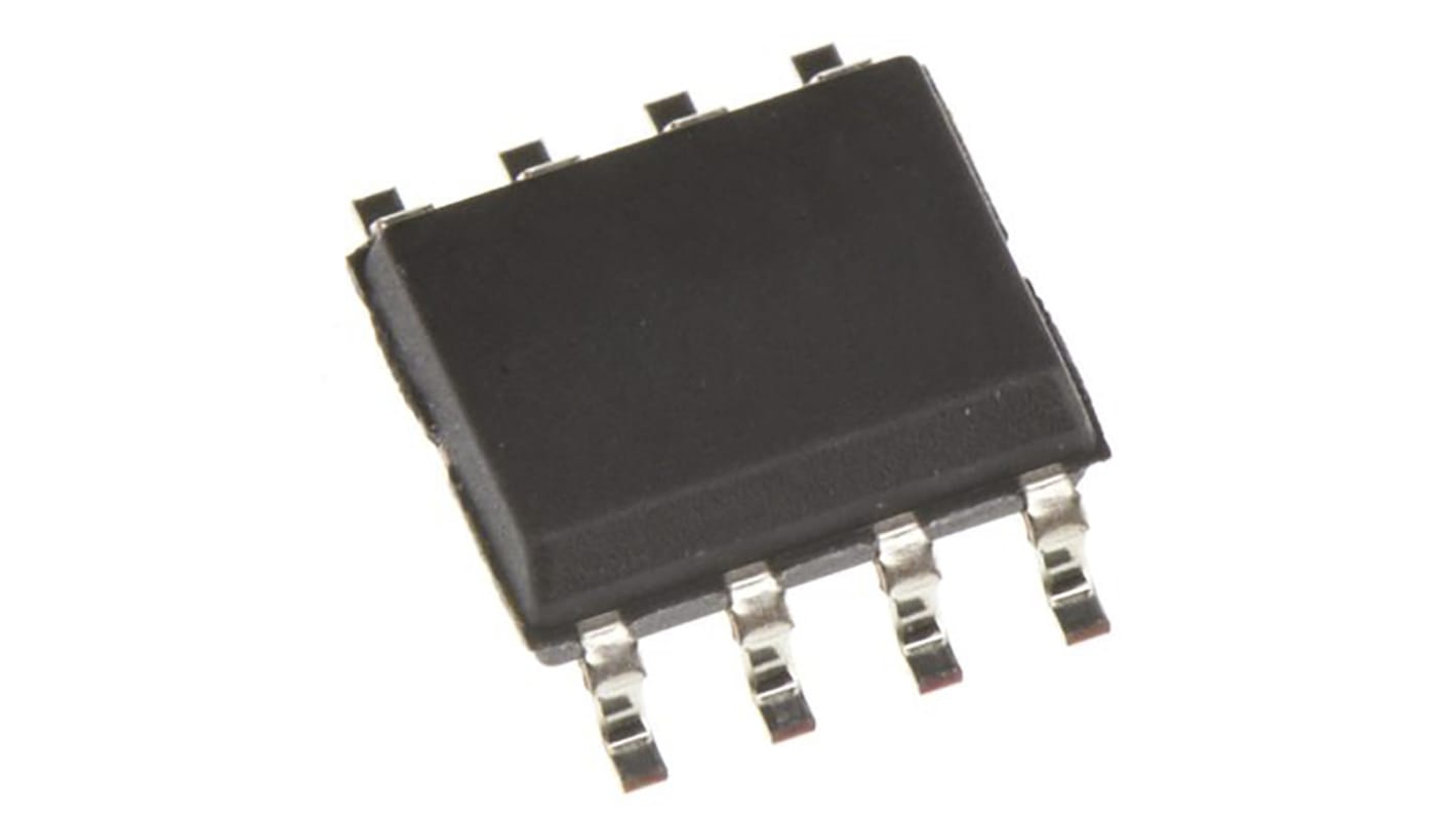
Infineon CY2302SXI-1 PLL Clock Buffer 8-Pin SOIC
- RS Stock No.:
- 194-8997
- Mfr. Part No.:
- CY2302SXI-1
- Manufacturer:
- Infineon

This image is representative of the product range
Bulk discount available
Subtotal (1 tube of 97 units)*
PHP42,655.362
(exc. VAT)
PHP47,774.052
(inc. VAT)
FREE delivery for orders over ₱3,000.00
Temporarily out of stock
- Shipping from October 22, 2026
Need more? Click ‘Check delivery dates’ to find extra stock and lead times.
Units | Per Unit | Per Tube* |
|---|---|---|
| 97 - 97 | PHP439.746 | PHP42,655.36 |
| 194 - 194 | PHP426.554 | PHP41,375.74 |
| 291 - 485 | PHP409.492 | PHP39,720.72 |
| 582 - 970 | PHP389.017 | PHP37,734.65 |
| 1067 + | PHP365.676 | PHP35,470.57 |
*price indicative
- RS Stock No.:
- 194-8997
- Mfr. Part No.:
- CY2302SXI-1
- Manufacturer:
- Infineon
Specifications
Technical data sheets
Legislation and Compliance
Product Details
Find similar products by selecting one or more attributes.
Select all | Attribute | Value |
|---|---|---|
| Brand | Infineon | |
| Product Type | PLL Clock Buffer | |
| Maximum Input Frequency | 133MHz | |
| Package Type | SOIC | |
| Pin Count | 8 | |
| Minimum Operating Temperature | -40°C | |
| Maximum Operating Temperature | 85°C | |
| Height | 1.47mm | |
| Length | 4.97mm | |
| Select all | ||
|---|---|---|
Brand Infineon | ||
Product Type PLL Clock Buffer | ||
Maximum Input Frequency 133MHz | ||
Package Type SOIC | ||
Pin Count 8 | ||
Minimum Operating Temperature -40°C | ||
Maximum Operating Temperature 85°C | ||
Height 1.47mm | ||
Length 4.97mm | ||
The CY2302 is a two-output zero delay buffer and frequency multiplier. It provides an external feedback path allowing maximum flexibility when implementing the Zero Delay feature.
91 ps typical jitter OUT2
200 ps typical jitter OUT1
65 ps typical output-to-output skew
90 ps typical propagation delay
Voltage range: 3.3 V ± 5%, or 5 V ± 10%
Output frequency range: 5 MHz to 133 MHz
Two outputs
Configuration options allow various multiplications of the reference frequency
Available in 8-pin SOIC package
Related links
- Infineon CY2302SXI-1 PLL Clock Buffer 8-Pin SOIC
- Infineon CY2304SXI-1 PLL Clock Buffer 8-Pin SOIC
- onsemi PLL Clock Buffer 8-Pin SOIC
- onsemi MC100LVEP11DG PLL Clock Buffer 8-Pin SOIC
- onsemi NB3N551DG PLL Clock Buffer 8-Pin SOIC
- onsemi MC100LVEL11DG PLL Clock Buffer 8-Pin SOIC
- onsemi NB2304AI1HDG PLL Clock Buffer 8-Pin SOIC
- onsemi NB3L553DG PLL Clock Buffer 8-Pin SOIC
